Analyzing a Unrecoverable Data Recovery Case
8GB CompactFlash Card
Controller Specs
4 Channels, 2-plane and interleave support for performance. Block level addressing
NAND
4 x Samsung K9LBG08U0D (16Gbits / 1CE Bank)
2Bit-MLC, 4 Planes (inconclusive)
4K Pages/512K Block Size[/one_third] [one_third_last] Interleaves
4-way byte Interleave.
Two plane operation (neighboring block).
Two plane operation (top/bottom half).
Final block size: 8MBytes.
[/one_third_last] [clear]
Controller
According to the product brief the controller has four channels with support for up to eight CE pins per channel. I found what looks like a block map overlay used for bad block mapping on each channel. It appears each of the four channels can operate independently however the controller manufacture chose to do a parallel 4-way byte interleave between all channels.
Design wise, I can see this being a simple implementation that spreads wear evenly across all four NAND chips however after factoring in interleaves the page size is 64Kbytes which as the product brief explains is great for DSLR’s that write long sequential blocks of data but for small random writes I suspect there would be a huge performance loss.
Interleaves
4 Way Byte Interleave
A parallel 4-way byte interleave on four channels acts similar to a RAID0 stripe in that you get quadruple the throughput. For writing large amounts of sequential data you’ll see a performance gain however if you’re not writing full pages worth of data you’re effectively loosing performance by hogging the bus for a partial 16KByte write.
[custom_frame_left shadow=”on”] [/custom_frame_left]
A 4-Way Byte Interleave merges data from four separate NAND chips (or CE’s). Typically the addresses are parallel (eg: block 200, 200, 200, 200) however this controller supports remapping so that if one of the parallel blocks is bad it’s remapped to a spare block (eg: block 100, 200, 200, 200). Similar to a RAID0, if one of the chips suffers a catastrophic failure the data across the remaining chips is generally useless (ie: every fourth byte is lost).
[/custom_frame_left]
A 4-Way Byte Interleave merges data from four separate NAND chips (or CE’s). Typically the addresses are parallel (eg: block 200, 200, 200, 200) however this controller supports remapping so that if one of the parallel blocks is bad it’s remapped to a spare block (eg: block 100, 200, 200, 200). Similar to a RAID0, if one of the chips suffers a catastrophic failure the data across the remaining chips is generally useless (ie: every fourth byte is lost).[clear]
Two Plane Operation (neighboring block)
In liegeman’s terms within a NAND chip is a built in mechanism for a RAID0 stripe. Modern NAND chips typically have two storage planes that share a single CE pin. While faster it’s not twice as fast as claimed by some NAND manufactures, random 4K IOPS also suffer.
[custom_frame_center shadow=”on”]
 [/custom_frame_center][clear]
[custom_frame_right shadow=”on”]
[/custom_frame_center][clear]
[custom_frame_right shadow=”on”] [/custom_frame_right]Most two plane operations interleave in parallel against the neighboring storage plane, some early implementations interleave sequentially against the top and bottom half’s of the chip. If read sequentially without two plane operations each plane presents itself as either an even or odd block.[clear]
Two Plane Operation (top/bottom half)
[custom_frame_right shadow=”on”] [/custom_frame_right]I assume this is what the manufacture was referencing when they listed “additional interleave” as a performance feature. A two plane interleave is performed on the second half of data then concatenated with the first two plane interleave. The datasheet is inconclusive but the NAND chip appears to have four planes, two at the first half of the chip and two on the bottom half.
[clear]
Error Correcting Code (ECC)
[custom_frame_left shadow=”on”]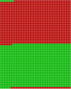 [/custom_frame_left]Now we get to see why recovery isn’t possible. Here is the ECC map for chip #1, each tiny square represents one sector (green = good, red = corrupt), the large green and red groupings of sectors represent blocks in plane 0 and plane 1. Due to the 4-Way byte interleave the corrupt data from chip #1 plane 1 is interleaved with all the data, essentially for every 64KBytes of data, 16KBytes is corrupt.
Now what’s strange is that the bottom half of the NAND chip is in perfect condition, combined this with the controller interleaving and concatenating data from the bottom half of the chip leads me to believe this Samsung NAND chip has four planes.
[clear]Diagnoses
Catastrophic failure in plane #1 on NAND Chip #1