NAND Read Retry for Data Recovery
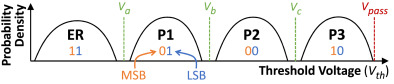 In addition to many of the common methods to improve NAND reliability and performance (eg: wear leveling, error correction code, etc) another common method we’re seeing is the inclusion of Read Retry (Voltage Sensitivity) registers. These registers appear to change NAND voltage gate sensitivity to improve the conditions for readability within a NAND page. Basically, raising or lowing the threshold for what is considered a 0 or 1 after degradation of a NAND cell from the loss of electrons.
While technically not a new technology, many Sandisk/Toshiba TLC chips and some from Hynix (eg: ad de 94 d2), Samsung (eg: ec d7 98 ca) NAND chips implemented this years ago, we are seeing this technology relied upon heavily in 3D/4D NAND chips from Intel, Samsung, SK Hynix to the point where without them it is almost impossible to get a read of the chip sufficient to be corrected by ECC.
TLC NAND is organized into planes, blocks, pages, and lower, middle, upper sub-pages. In my research each sub-page has its own sensitivity register(s) which can be adjusted dynamically depending on the outcome of the last page read. If the controller is unable to correct ECC damage to a specific page (page % 3 = sub-page) or group of sub-pages the controller will execute a special command sequence that will allow modification of the internal voltage sensitivity registers and re-read the offending page.
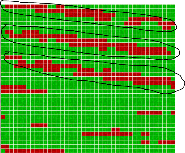
In the example below the lower sub-page is read correctly however the middle and upper sub pages aren’t. By modifying the read retry register for the middle and upper sub-pages it is likely possible that the data can be read without issue.

Another interesting effect are even and odd planes having different Read Retry values which must be accounted for during multi-plane operations.
Here is a real-world example of the lower sub-page read retry value needing adjustment. You can see bands with uncorrectable ECC errors. Modifying the value for the lower sub-page will likely result in a good read.
There is generally a two-year lag between when new technology comes out and when it is seen in-shop for data recovery. 3D/4D NAND will be the new standard and the data recovery industry will likely be inundated with NAND chips coming out that might appear unrecoverable (ie: too many bit errors) due to internal NAND failure but are actually recoverable with the use of Read Retry (voltage sensitivity) codes. Many data recovery platforms are currently unable to read these chips and instead label them as commonly defective chips.
Instead platforms are relying on crude dictionary attacks to read NAND chips with limited success instead of fully exploiting the ability to scan the full range of retry values. Read Retry must be looked at granularly at the sub-page level not at the block or NAND level as data recovery platforms currently do.
Every manufacture and every model of chip (ie: different ID) appears to have its own Read Retry implementation. Successfully mapping out the appropriate registers on one chip doesn’t guarantee success on others.